Pages

Wednesday, March 25, 2015

EVPN (RFC 7432) Explained

EVPN (RFC 7432) Explained

EVPN or Ethernet VPN is a new standard that has finally been given an RFC number. Many vendors are already working on implementing this standard since the early draft versions and even before that Juniper already used the same technology in it’s Qfabric product. RFC 7432 was previously known as: draft-ietf-l2vpn-evpn.

EVPN is initially targeted as Data Center Interconnect technology, but is now deployed within Data Center Fabric networks as well to use within a DC. In this blog I will explain why to use it, how the features work and finally which Juniper products support it

Sunday, March 22, 2015

The Q5 ASIC - new custom silicon from Juniper Networks

QFX10000 - a no compromise switching system with innovation in silicon and memory technology

Typically, networking silicon and systems in general can be split across two categories.
High I/O Scale & shallow memory. In order to break the 200-300Gbps throughput barrier on the switch silicon and build silicon that can provide a much higher forwarding throughput that is upwards of 1Tbps, typically a silicon is designed as a “Switch on Chip (SOC)”. What that means is all the forwarding logic as well as buffers to store the incoming & outgoing packets in the system are self-contained and stored natively on the silicon and not on memory external to the silicon. The reason it is done is due to the memory-to-asic bandwidth constraints. The moment memory to store the packets incoming & outgoing of the system is external to the forwarding silicon, the silicon throughput will immediately be gated by that interface that exists between the silicon and the memory. As a result, in order to build systems with very high I/O capacity, a compromise is often made to have very shallow buffers and lookup capacity that is natively available on the silicon itself and not have that slow speed memory to silicon interface. This places certain constraints on the network designs. An example of such a constraint would be that systems designed with an SOC cannot be used in data center edge applications as data center edge application requires full FIB capacity and an SOC would typically not have enough memory to hold a full routing table. Another example would be where applications could be bursty in nature or application could not respond to congestion events in the network by flow controlling themselves and require a fairly deep amount of buffering to be provided by the network. Typically, an SOC of 1Tbps would have about 10MB-24MB or so of buffer shared across all ports and a small amount of tcam for table lookups.

How 3D Memories Help Networking ASICs to be Energy Efficient


Powerful but “Green” - How 3D Memories Help Networking ASICs to be Energy Efficient
When I was on stage at the NANOG 49 in San Francisco (Abstract) in June of 2010, explaining the importance of memories to networking, lamenting the slow pace of progress of the memory technologies in the past decade, and urging the memory industry to step up to the plate and break the memory bottleneck, little did I know that the breakthrough was already in the works secretly in a lab in Micron’s Boise, Idaho, headquarters, just 600 miles away. When Micron representatives presented the technology, which eventually led to the creation of Hybrid Memory Cube (HMC), to Juniper later that year, it was like a marriage made in heaven. Both teams immediately recognized the mutual benefits and sprang into action. The rest, as they said, is history.

Fast forward four and a half years. Last week, we announced products and services based on the ExpressPlus and Q5 ASICs, with HMC as the companion memory. With a number of other innovations including virtual output queueing, efficient lookups, and high performance packet filter technology, the ExpressPlus and Q5 ASICs are the industry’s first 500Gbps (1Tbps half duplex) single chip ASICs with large delay bandwidth buffers and large lookup tables, and with breakthrough power efficiency to enable high density systems.

The HMC is made of multiple DRAM “layers” stacked together in a 3-D fashion, communicating with each other and to the base logic layer by ways of Through-Silicon-Vias (TSVs), as illustrated in the following diagram. The TSVs are denser and shorter than the regular wires in conventional DDR3/4 memories, and therefore can support much higher bandwidth with lower latency and lower power. In addition, the base logic layer implements SERDES IOs that are up to 7 times faster than the IOs in conventional memories, which leads to considerably fewer IO pins for the ASICs to communicate with the external memories.

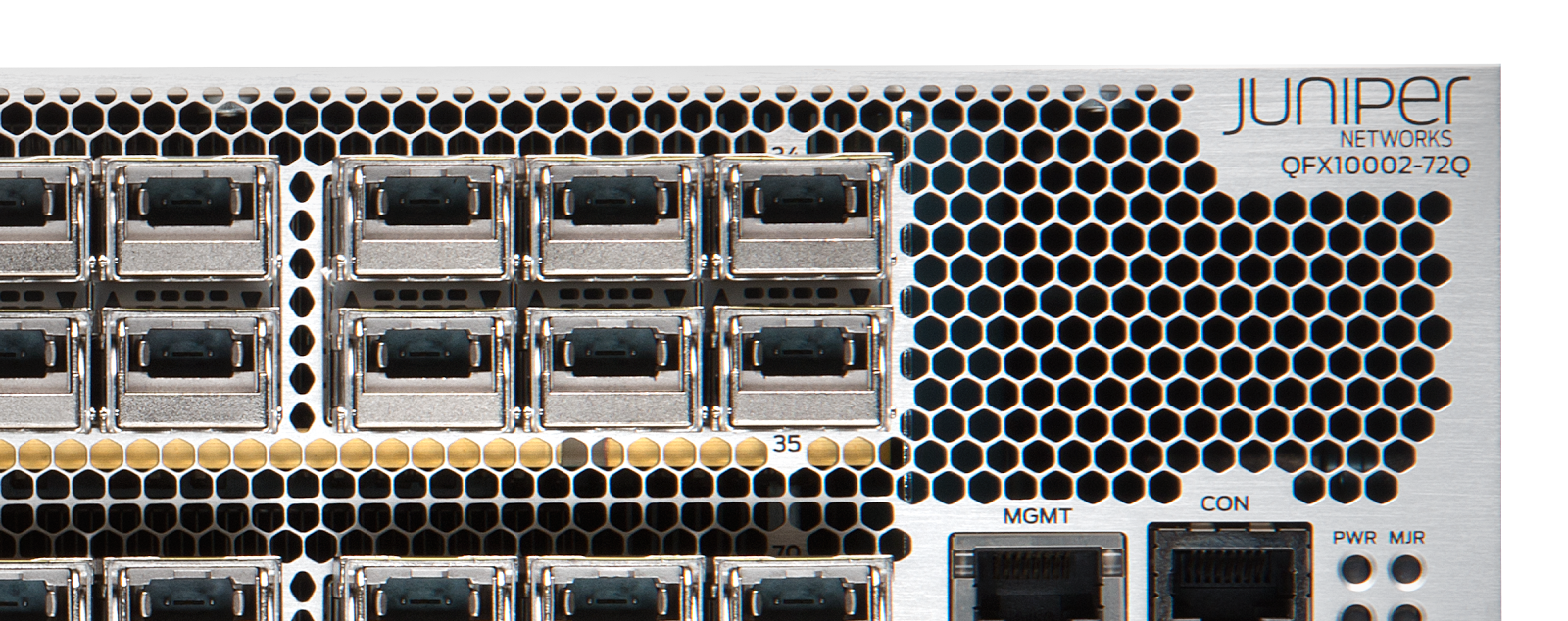
Juniper QFX10002 Technical Overview


This blog post will focus on the new Juniper QFX10002. Everything mentioned in this blog is applicable to the larger Juniper QFX10008 and QFX10016. The only differences are port density between the different models of the QFX10000.